Improving semiconductor fabrication
- Semiconductor
- Absorbance
- High Sensitivity Spectrometers
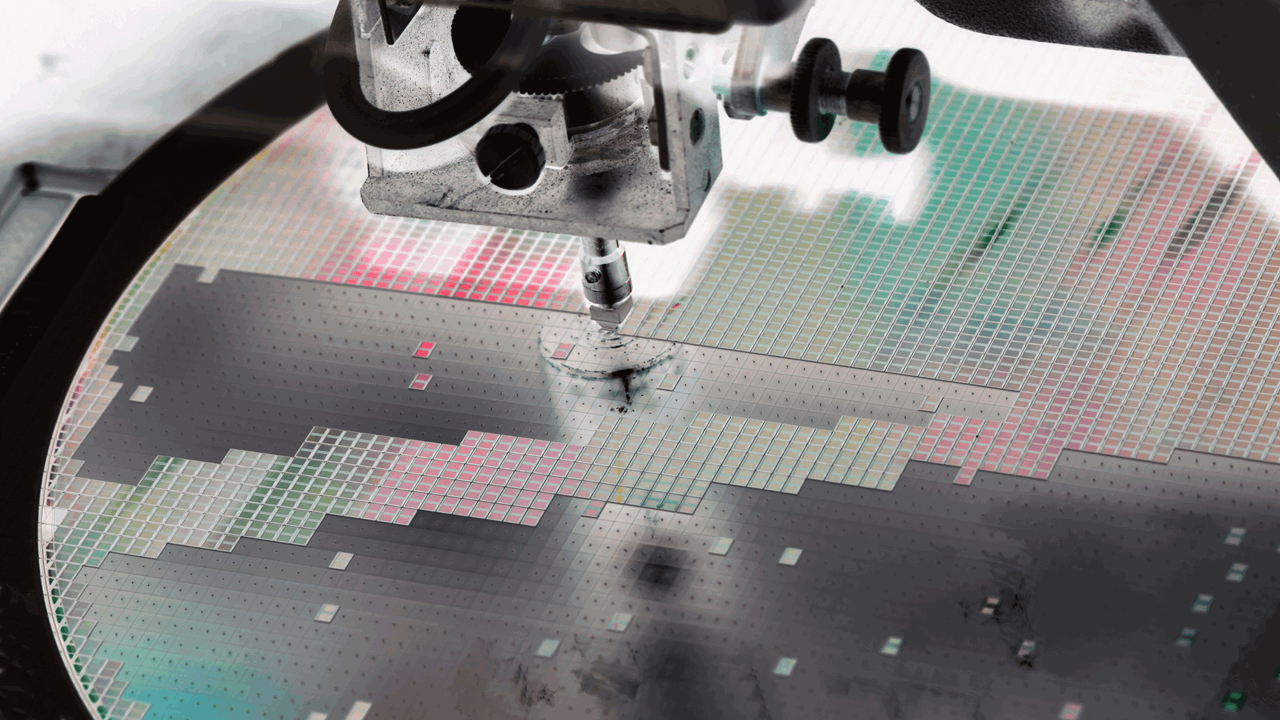
Ocean Insight partnered with a leading innovator in plasma-etching technologies, to explore full-spectrum plasma monitoring solutions suitable for detecting critical wafer etch endpoints
With the rapidly increasing global demand for semiconductors, the industry is well-positioned to invest in cost-saving process improvements and the development of increasingly sophisticated semiconductor designs and recipes. To feed today’s technology boom and weather the expanding market, semiconductor foundries require quantitative, accurate and high-speed process measurements.
Semiconductors and microelectromechanical systems (MEMS) are reaching design limitations, where further improvement via size reduction or increased speed is nearly impossible. Instead, manufacturers are focusing on wafer quality, repeatability and overall yield, as well as increased production capacity. The goal is to meet the growing demand for smart electronics while maintaining production costs and keeping prices competitive.

Rapid analysis of faint plasma or wafer spectra can help to perfect etch process parameters while improving wafer quality. Spectrometer-based plasma measurements paired with powerful software can account for the changing state of plasma, chamber and viewport conditions, and be sensitive to the faintest signals from deep etches or thin design features.
Spectroscopy helps to make endpoint detection more precise, which makes it possible to design more intricate wafer shapes and patterns. Because manufacturers can more accurately stop and start production processes, smaller features can be made with fewer errors and less unusable space on the wafer. Also, as endpoint detection becomes more accurate, thinner layers of different materials can be used, even as they generate faint, difficult to discern spectral signatures and more closely aligned peaks.
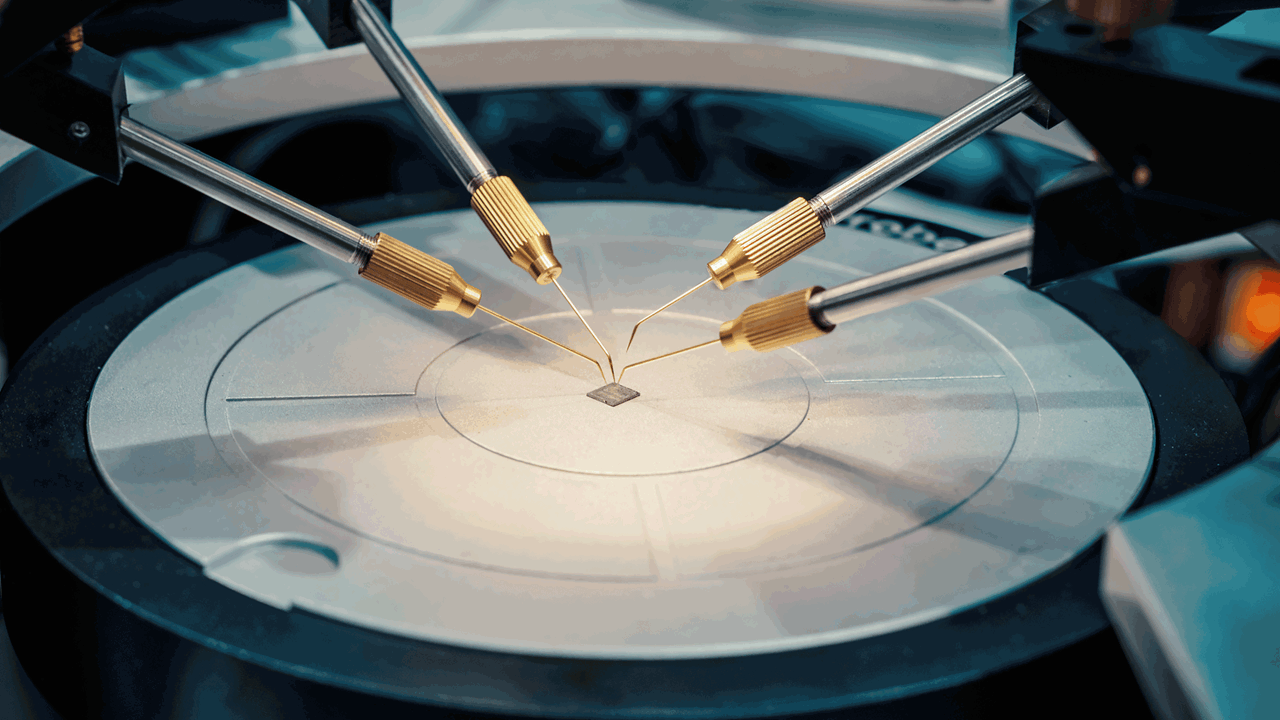
Ocean Insight teamed with a leading supplier of equipment to the semiconductor industry to advance endpoint detection techniques. We customized spectrometers (the Ocean SR2 and Ocean HDX are good options for plasma monitoring applications) to provide fast, high sensitivity, pinpoint resolution and versatile connection capabilities needed in semiconductor fabrication.
With Ocean Insight hardware and support, the equipment supplier continues to improve and refine the etching technologies it offers to the semiconductor industry. Its leadership in plasma-processing and advanced packaging solutions supports emerging technologies related to wireless devices, photonics, solid state lighting and MEMS devices.
Our world-class experts are available to help find answers to your toughest questions.