Are you ready to explore how Ocean Optics can help you?
Our world-class experts are available to help find answers to your toughest questions.
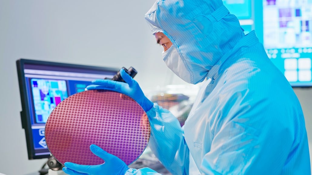
From plasma monitoring and plasma etching to endpoint detection in semiconductor processing, we offer optical sensing solutions to help with manufacturing processes. The result? Accelerated time to market, higher process yields, and improved product quality.
Learn how spectral tools boost yields and ensure device quality.
Spectroscopy-based sensors can be utilized not only in semiconductor deposition and etching processes, but also for chamber sterilization. These tools help to optimize wafer yields and quality.
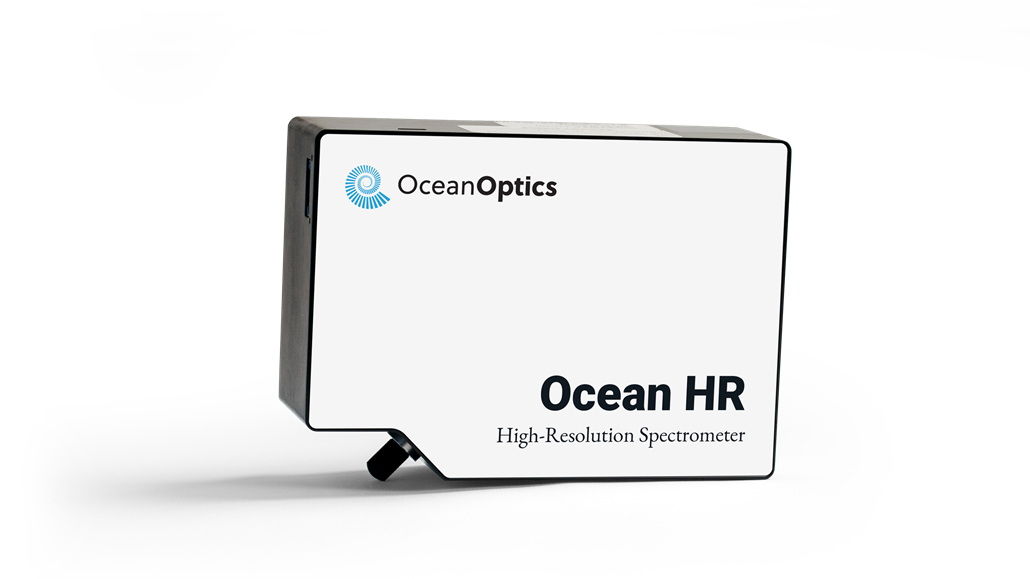
High resolution and thermal stability with rapid data acquisition speed
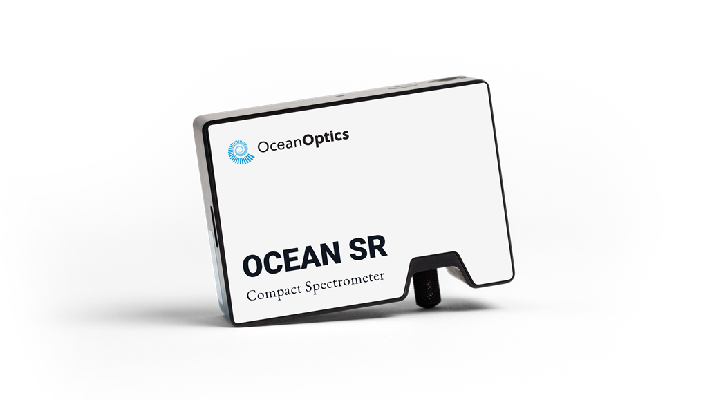
Fast acquisition speed and high SNR
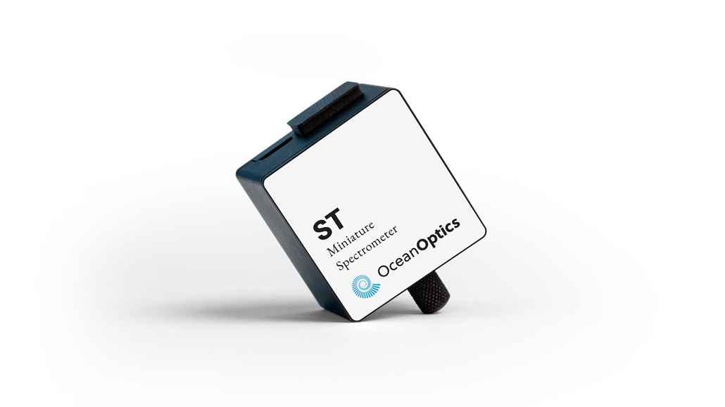
Ultra-compact device with great UV response and high SNR
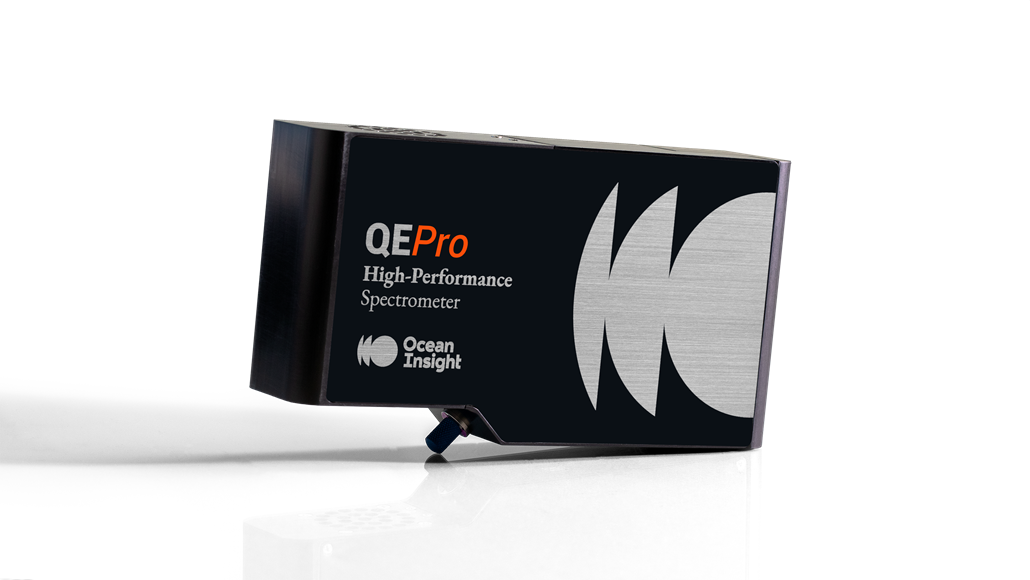
High-sensitivity, back-thinned CCD spectrometer
Our world-class experts are available to help find answers to your toughest questions.